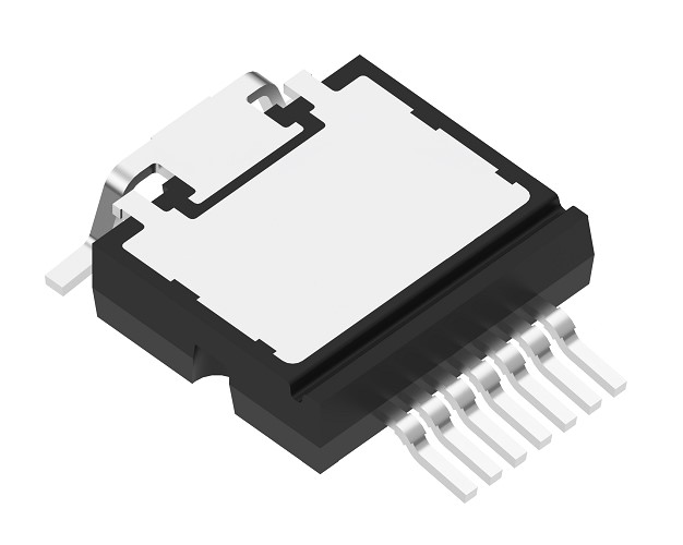
Silicon Carbide Schottky diode in a TSPAK plastic package, featured with top side cooling structure, designed for high frequency, high efficiency systems.
- Top side cooling structure
- Highly stable switching performance
- High forward surge capability IFSM
- Extremely fast reverse recovery time
- Superior in efficiency to Silicon Diode alternatives
- Reduced losses in associated MOSFET
- Reduced EMI
- Reduced cooling requirements
- RoHS compliant
- High junction operating temperature capability (Tj(max) = 175 °C)
- Switching mode power supplies
- UPS & energy storage systems
- PV inverter and MPPT circuit
- Battery formation systems
- EV chargers
- Motor Drives
| Type Number | Symbol | Parameter | Conditions | Min | Typ/Nom | Max | Unit |
| WNSC2D401200TB | VRRM | repetitive peak reverse voltage | 1200 | V | |||
| IF(AV) | average forward current | Tmb ≤ 118 °C; DC | 40 | A | |||
| Tj | junction temperature | 175 | °C | ||||
| VF | forward voltage | IF = 40 A; Tj = 25 °C | 1.42 | 1.60 | V | ||
| IF = 40 A; Tj = 150 °C | 1.90 | 2.30 | V | ||||
| Qr | reverse charge | IF = 40 A; VR = 400 V; dIF/dt = 500 A/µs; Tj = 25 °C | 99 | nC |
| Type number | Package | Packing | Product status | Marking | Orderable part number | Ordering code (12NC) |
|---|---|---|---|---|---|---|
| WNSC2D401200TB |
TSPAK | REEL 13\" Q1/T1 *STANDARD MARK SMD" | Volume production | Standard Marking | WNSC2D401200TB6J | 9340 740 03118 |
| Type number | Ordering code (12NC) | Orderable part number | Region | Distributor | Order sample |
|---|---|---|---|---|---|
| WNSC2D401200TB | 9340 740 03118 | WNSC2D401200TB6J | NA | NA |
| Chemical content | Orderable part number | Type number | RoHS / RHF | Leadfree conversion date | MSL | MSL LF |
|---|---|---|---|---|---|---|
| WNSC2D401200TB | WNSC2D401200TB6J | WNSC2D401200TB |  |
Chemical Content - WNSC2D401200TB
Disclaimer
All information in this document is furnished for exploratory or indicative purposes only. All information in this document is believed to be accurate and reliable. However, WeEn Semiconductors does not give any representations or warranties as to the accuracy or completeness of such information and shall have no liability for the consequences of use of such information. WeEn Semiconductors may make changes to information published in this document at any time and without notice. Minor deviations may occur in the products from different manufacturing location. This document supersedes and replaces all information supplied prior to the publication hereof. Nothing in this document may be interpreted or construed as an offer to sell products that is open for acceptance or the grant, conveyance or implication of any license under any copyrights, patents or other industrial or intellectual property rights.