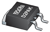
Planar passivated high commutation three quadrant triac in a TO263 (D2PAK) surface mountable plastic package intended for use in circuits where high static and dynamic dV/dt and high dIT/dt can occur. This triac will commutate the full RMS current at the maximum rated junction temperature (Tj(max) = 150 °C) without the aid of a snubber. It is used in applications where high junction operating temperature capability is required.
- 3Q technology for improved noise immunity
- High commutation capability with maximum false trigger immunity
- High junction operating temperature capability (Tj(max) = 150 °C)
- High voltage capability
- High current capability
- Less sensitive gate for highest noise immunity
- Triggering in three quadrants only
- Very high immunity to false turn-on by dV/dt and fast transients
- Surface mountable plastic package
- Package is RoHS compliant
- Heating controls
- High power motor control
- High power switching
- Applications subject to high temperature (Tj(max) = 150 °C)
| Type Number | Symbol | Parameter | Conditions | Min | Typ/Nom | Max | Unit |
| BTA330B-800BT | VDRM | repetitive peak off-state voltage | 800 | V | |||
| IT(RMS) | RMS on-state current | full sine wave; Tmb ≤ 120 °C; | 30 | A | |||
| ITSM | non-repetitive peak on-state current |
full sine wave; Tj(init) = 25 °C; tp = 20 ms; | 270 | A | |||
| full sine wave; Tj(init) = 25 °C; tp = 16.7 ms | 297 | A | |||||
| Tj | junction temperature | 150 | °C | ||||
| IGT | gate trigger current | VD = 12 V; IT = 0.1 A; T2+ G+;Tj = 25 °C; | 50 | mA | |||
| VD = 12 V; IT = 0.1 A; T2+ G-;Tj = 25 °C; | 50 | mA | |||||
| VD = 12 V; IT = 0.1 A; T2- G-;Tj = 25 °C; | 50 | mA | |||||
| IL | latching current | VD = 12 V; IG = 0.1 A; T2+ G+; Tj = 25 °C; |
80 | mA | |||
| VD = 12 V; IG = 0.1 A; T2+ G-; Tj = 25 °C; |
100 | mA | |||||
| VD = 12 V; IG = 0.1 A; T2- G-; Tj = 25 °C; |
80 | mA | |||||
| IH | holding current | VD = 12 V; Tj = 25 °C; | 75 | mA | |||
| VT | on-state voltage | IT = 42 A; Tj = 25 °C; | 1.2 | 1.5 | V | ||
| dVD/dt | rate of rise of off-state voltage | VDM = 536 V; Tj = 125 °C; (VDM = 67% of VDRM); exponential waveform; gate open circuit |
4000 | V/µs | |||
| VDM = 536 V; Tj = 150 °C; (VDM = 67% of VDRM); exponential waveform; gate open circuit |
2000 | V/µs | |||||
| dIcom/dt | rate of change of commutating current |
VD = 400 V; Tj = 125 °C; IT(RMS) = 30 A; dVcom/dt = 20 V/μs; (snubberless condition); gate open circuit |
20 | A/ms | |||
| VD = 400 V; Tj = 150 °C; IT(RMS) = 30 A; dVcom/dt = 20 V/μs; (snubberless condition); gate open circuit |
15 | A/ms |
| Type number | Package | Packing | Product status | Marking | Orderable part number | Ordering code (12NC) |
|---|---|---|---|---|---|---|
| BTA330B-800BT |  TO263 |
STANDARD MARK SMD | Volume production | Standard Marking | BTA330B-800BTJ | 9340 721 75118 |
| Type number | Ordering code (12NC) | Orderable part number | Region | Distributor | Order sample |
|---|---|---|---|---|---|
| BTA330B-800BT | 9340 721 75118 | BTA330B-800BTJ | NA | NA |
| Chemical content | Orderable part number | Type number | RoHS / RHF | Leadfree conversion date | MSL | MSL LF |
|---|---|---|---|---|---|---|
| BTA330B-800BT | BTA330B-800BTJ | BTA330B-800BT | 1 | 1 |
Chemical Content - BTA330B-800BT
As a proactive and sustainable company, WeEn Semiconductors has decided to publish chemical content information of its product portfolio through direct Internet access. With this information, we can provide data to our customers to facilitate any assessment regarding compliance to the RoHS directive and lead-free status. WeEn Semiconductors has set a standard in the semiconductor business with this detailed level of data, directly retrieved from its general product database. WeEn Semiconductors products are compliant to the EU Directives RoHS, ELV and the China RoHS.
Disclaimer
All information in this document is furnished for exploratory or indicative purposes only. All information in this document is believed to be accurate and reliable. However, WeEn Semiconductors does not give any representations or warranties as to the accuracy or completeness of such information and shall have no liability for the consequences of use of such information. WeEn Semiconductors may make changes to information published in this document at any time and without notice. Minor deviations may occur in the products from different manufacturing location. This document supersedes and replaces all information supplied prior to the publication hereof. Nothing in this document may be interpreted or construed as an offer to sell products that is open for acceptance or the grant, conveyance or implication of any license under any copyrights, patents or other industrial or intellectual property rights.


