In our modern society, electricity is becoming an ever more important resource of energy. Common examples of energy users and producers are computing equipment (desktop computer, tablets, but also server farms including un-interruptible power supplies), communication equipment (mobile phones, base stations), electric vehicles (traction and battery charging), PV energy harvesting equipment (solar energy farms) and wind turbines (wind farms). Handling the electric energy efficiently has become essential; 1200V diodes can help.
High voltage
It is a well-known fact in electric energy transfer that Ohmic losses in low voltage systems have a larger impact on efficiency than in high voltage systems. It is for that reason that new standards for mobile phone and tablet charging have been developed (USB-PD) that allow these devices to be charged from 9V, 12V or even 20V sources, where in the early days 5V was the standard.
Of course, mobile phones and tablets are more or less low power systems (in the order of 1 to 10 Watts), but a similar tendency can be observed in higher power systems (1 kW and above). High power electric power conversion systems like UPS, PV inverters and EV chargers are commonly built using DC/DC converter building blocks like Boost/Flyback Converters, Buck/Forward Converters and Resonant Converters. Flyback and Forward Converters are basically the isolated counterparts of the Boost and the Buck Converter respectively.
Traditionally the highest DC voltage levels in this kind of systems used to be around 400V. In many new high power systems an internal DC voltage of 700V or above is used in order to benefit from efficiency advantages that can more easily be realized by using higher voltage. Basically for the same reason why many modern mobile phones use USB-PD voltage levels of in the order of 12V and not the traditional 5V USB level.
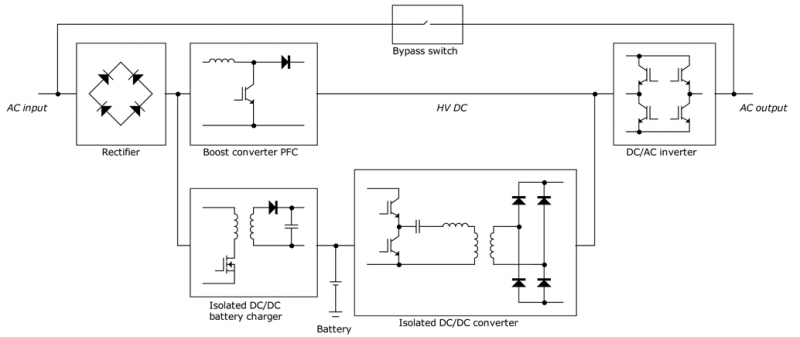
Figure 1: Block diagram of a UPS system with various DC/DC building blocks
Hard switching, soft switching and power loss resulting from diode behavior
When it comes to the switching behavior of DC/DC converters, there’s essentially just hard switching and soft switching. Bipolar pn-junction diodes behave differently under hard switching and soft switching circumstances. This can be illustrated by examining the operation of a boost converter in continuous conduction mode (CCM) and of an LLC resonant converter. The CCM boost converter is essentially hard switching, the LLC resonant converter is essentially soft switching.
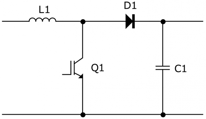
Figure 2: Principle diagram of a boost converter
Hard switching
A CCM boost converter is often used as the power factor correction (PFC) circuit in a power converter system. When, at time t1, switch Q1 is closed the current in inductor L1 (IL1) builds up while the current in diode D1 (ID1) stops to flow. When Q1 is opened at time t2, the current starts to flow through the diode. At the moment that D1 must start to conduct the current (at time t2) only a low concentration of charge carriers (electrons and holes) is present in the drift region of the diode. That makes the initial impedance of the diode relatively high, which results in a high voltage drop (Vfr) across the diode. After a certain time (tfr – mostly in the order of 10 to 100 ns) sufficient charge carriers have been injected into the drift region, the impedance of the diode drops dramatically and the voltage drop across the diode is reduced to the static VF level for the specific forward current. The energy loss due to diode switch-on (switch-on loss) can be approximated by:
![]()
The energy Esw-on is completely dissipated in the diode itself.
After switching on, the current through the diode continues to flow and ramps down. Ramp continues until switch Q1 is closed again. The energy dissipation during the diode coductuction period is:

Which can be estimated to be approximately equal to:
![]()
Where VF and IF are the average VF and IF levels respectively. All conduction loss is dissipated in the diode.
At the moment Q1 is closed the sequence repeats.
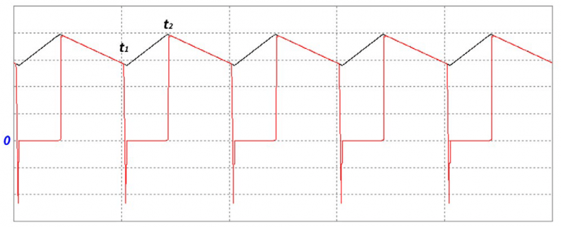
Figure 3: Current waveform in the diode of a CCM boost converter (simulated); black = IL1, red = ID1
The current that flows in diode D1 at the moment it’s being switched off (t1) significantly deviates from zero. Under that circumstance a bipolar diode cannot block the current instantaneously. In a bipolar diode the stored charge in the drift region must be removed before the diode can block the current flow. The reverse current associated with the extraction of the stored charge can clearly be recognized in figure 3. Removal of the stored charge (Qs) leads to power loss: switch-off loss (Esw-off). The power loss associated with switching off is proportional to the voltage trajectory that the stored charge need to travel; in a normal boost converter that voltage trajectory is equal to the output voltage of the boost converter (Vout); namely the stored charge was initially at Vout level and is ‘transported’ to ground potential (0 V) because Q1 is closed.

The stored charge Qs is the product of the current flowing in the diode (IF) and the (ambipolar) charge carrier lifetime Ta
![]()
Combining equations (3) and (4), and knowing that switch-off occurs at t1, the expression for the switch-off loss is:

The energy Esw-off is normally only partially dissipated in the diode itself; generally a lot of the energy will be dissipated in switch Q1.
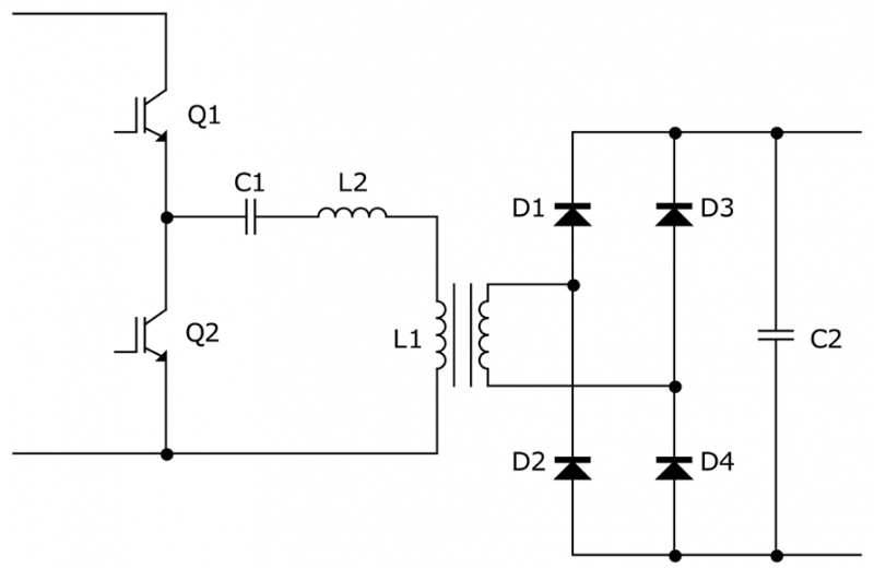
Figure 4: Principle diagram of an LLC resonant converter
TThe ambipolar charge carrier lifetime Ta is not a constant; lifetime decreases with current density in the silicon device. That makes it interesting to consider to use a smaller diode in order to reduce power loss in the system as a whole, especially when switching loss happens to be already dominant over conduction loss. Although the conduction loss will increase when a smaller diode is applied in an application, that loss may be more than compensated by the reduction of switching loss. See also the text box “Conduction loss versus switching loss”.
Charge carrier lifetime increases with temperature. Therefore it makes sense to try to keep the operating temperature of a bipolar diode low in order to keep switching loss low.
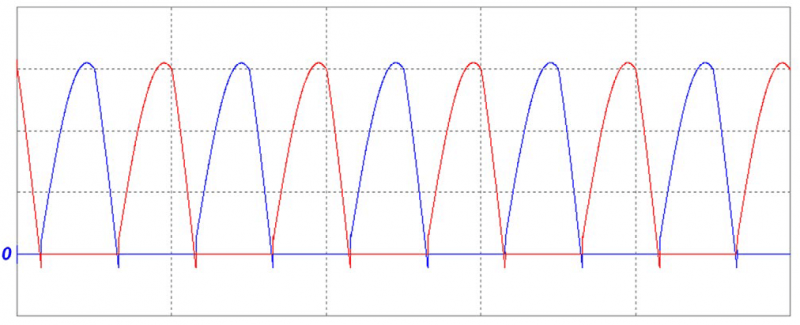
Figure 5: Current waveforms in the diodes of an LLC resonant converter (simulated); blue = ID1 and ID4, red = ID2 and ID3
Soft switching
An LLC resonant converter can often be found as a building block in a UPS or PV inverter. The switches Q1 and Q2, together with L1 (the magnetization inductance of the transformer), L2 (the leakage inductance of the transformer) and C1 (the series capacitance of resonating circuit) create a sinusoidal (or piecewise sinusoidal) current flowing out of the secondary side of the transformer. That sinusoidal current is rectified by the diode bridge (D1, D2, D3, D4), causing a DC voltage to result across the output buffer capacitor C2. The current that flows in diode pair D1 and D4 (and in the pair D2 and D3) is essentially zero when the diodes are switching on and switching off. Because the diodes switch on at zero-crossing, diode turn-on losses are much lower than in a hard switching topology – the Vfr voltage overshoot is much lower and sometimes not even detectable. For switch-on power loss the same equation (1) applies as for a hard switching topology, but in a soft switching topology IF is close to zero, so the switch-on losses are nearly zero.
Conduction loss versus switching loss
In semiconductor switches (diodes, BJTs, MOSFETs, etc.) two aspects generally, determine the power loss: current conduction and switching. Conduction loss (on-state loss) can be reduced by making the semiconductor switch lager. Switching loss occurs because of change in the ‘charged state’ of a semiconductor switch: the most charge is involved in the transition, the higher the switching loss. Switching losses can be reduced by:
• Making the semiconductor switch smaller,
• Adapt the internal operation of the device in such a way that less Charge is involved in a switching transition. As a side effect this Adaption usually leads to higher conduction loss.
Switching loss is proportional to the switching frequency. When the switching frequency is low, conduction loss will nearly always de dominant; selecting the biggest device generally gives the lowest power loss. A high switching frequency, a trade-off must be made between conduction loss and switching loss arrive at minimum total power loss. In that case the optimum device will either be (1) a smaller switch or (2) a switch with adapted characteristics, or a combination of the two. Higher conduction loss must be tolerated to arrive at minimum total power loss.
Diode switch-off losses are also much lower because the forward current level is approaching zero when the diode needs to turn off. Again the same equation (3 or 5) applies, but IF is substantially lower than in a hard switching topology. So that makes switch-off losses much lower as well, which can easily be recognized in the diode’s reverse recovery current magnitude in figure 5 – the reverse recovery current only slightly drops below zero.
The main requirement for the diode is that it must be fast enough to keep pace with the switching frequency of the (LLC resonant) power converter.
One component in the energy loss cannot be avoided: conduction loss. Also in soft switching topologies the conduction loss is given by equation (2).
Because switching losses play a less significant role in soft switching topologies the same (ultrafast/hyperfast) bipolar diodes can be used up to much higher switching frequencies in soft switching topologies than in hard switching topologies.
1200V diodes
Hyperfast bipolar diodes need lifetime control in order to make them switch fast (see also the text box “Lifetime control”) – in principle there’s no fundamental difference between 600V diodes and 1200V diodes. But, compared to 600V diodes, 1200V diodes require a wider drift region/depletion region in order to cope with the 1200V reverse voltage. The consequence of that wider region is that stored charge extraction (at the moment that the diode should turn off) takes longer. In order to make a 1200V diode just as fast as a 600V diode, it needs the lifetime of the charge carriers to be reduced even further. This additional carrier lifetime reduction unfortunately also affects the forward voltage drop of the diode: VF will rise and consequently conduction loss will be higher. It is for this reason that 600V Hyperfast diodes have trr values specified in the order of 20 ns where 1200V Hyperfast diodes have trr values in the order of 60 ns.
Where picking the right balance between conduction loss and switching loss in 600V diodes was already a challenge, it is even more challenging for 1200V diodes.
Lifetime control
Semiconductor switches are either unipolar switches (like Schottky diodes and MOSFETs) or bipolar switches (like pn-junction diodes and BJTs). In a unipolar device only electrons or holes conduct the current, in a bipolar switch both electrons and holes conduct the current. One advantage of unipolar switches is that they can switch very quickly while the main advantage of bipolar devices is that they are better current conductors.
Through the so-called conductivity modulation phenomenon, a bipolar switch conducts the current much better than a unipolar switch for the same amount of silicon used.
However, conductivity modulation also has a disadvantage. When a bipolar device conducts, a high concentration of charge carriers (electrons and holes) is injected into the drift layer of the device (that’s what makes the device conduct so well). But, when the bipolar device needs to switch off, the excess charge carriers must first be removed before the device can start blocking the current: bipolar devices cannot switch-off instantaneously. Either one will have to wait until the excess electrons and holes In the drift layer have recombined spontaneously or one will have to extract the charge carriers actively. When extracted actively, a so-called reverse recovery current flows in a bipolar diode before the device actually blocks the current flow.
The charge concentration that can be injected into the drift layer depends on the lifetime of the charge carriers. In ‘normal’ silicon the effective lifetime of charge carriers is in the order of several microseconds. For standard 50 or 60 Hz rectifier diodes that charge carrier lifetime is no limitation for the diode’s operation. However, in bipolar diodes that need to switch at much higher frequency, lifetime control must be used to reduce the effective lifetime of the charge carriers.
Reduced charge carrier lifetime reduces the charge concentration in the drift layer of the diode. That makes the diode less well conducting in the on-state (higher VF), but it also makes it easier to extract the excess stored charge and it speeds-up spontaneous electron-hole recombination: the diode switches faster (lower trr). Charge carrier lifetime can be controlled by diffusing a low concentration of gold (Au-kill) or platinum (Pt-kill) into the silicon. The Au or Pt atoms will operate as recombination centers: they speed-up the recombination of electrons and holes.
Unfortunately, recombination centers operate as generation centers when the diode is in the off-state. This causes a fast Au-killed or Pt-killed diode to have a much higher leakage current than a slow “un-killed” diode; the faster the diode, the higher the leakage current. Furthermore, the leakage current increases with rising temperature which can lead to thermal runaway. A substantial difference between Au-killed and Pt-killed diodes, is that the Au-killed diodes have much higher leakage current than Ptkilled diodes at the same operating temperature. Where most Au-killed diodes cannot be used at an operating temperature above 150°C, Pt-killed diodes are able to operate at a temperature of 175°C or higher and are therefore a more reliable solution.
Leakage and high operating temperature capability
High reverse voltages across a bipolar diode’s terminals will cause a leakage current to flow. Hyperfast diodes need a high concentration of recombination centers (see also the text box “Lifetime control”) in order to give the device its fast switching properties, but unfortunately these recombination centers do also operate as generation centers that contribute to a higher leakage current. Furthermore, when the operating temperature of a Hyperfast diode rises the activity of the generation centers increases, which leads to higher leakage current. When a Hyperfast diode must be able to operate reliably at high temperature, it is essential that the leakage current does not rise to a level where the dissipation because of leakage could result in thermal runaway of the device. In order to achieve that a lifetime control method should be used that gives the Hyperfast diode these desired properties. The traditional so-called “Gold-kill” process does usually not allow the resulting Hyperfast diodes to be used above an operating temperature of 150 °C. An enhanced so-called “Platinum-kill” process delivers Hyperfast diodes that can be used up to temperatures of 175 °C and is therefore preferred for manufacturing Hyperfast low-leakage diodes that are capable of operating at high temperature. Using the right lifetime control and choosing the right balance between conduction losses and switching losses results in 1200V Hyperfast diodes that enables cost effective and efficient high power/ high voltage switched mode power conversion systems.
About WeEn Semiconductors
WeEn Semiconductors was established in 2016 as the continuation of NXP's Bipolar Power Business Line. WeEn Semiconductors Co., Ltd, is the global joint venture between NXP Semiconductors N.V. and Beijing JianGuang Asset Management Co. Ltd (JAC Capital). WeEn Semiconductors’ business and operations center is located in Shanghai, China.


