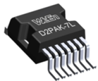
Silicon Carbide MOSFET in a TO263-7L plastic package, designed for high frequency, high efficiency systems.
- Kelvin source configuration
- Low specific on-resistance
- Optimized dynamic performance
- 0V turn-off VGS for simple gate driving
- 100% UIS Tested
- Easy to parallel
- RoHS compliant
- Automotive Qualified (AEC-Q101)
- Automotive on board chargers
- Automotive DC-DC converters
- Automotive electric compressor motor drives
- HV battery management systems
| Type Number | Symbol | Parameter | Conditions | Min | Typ | Max | Unit |
| WNSC2M75120B7-A | VDS | drain-source voltage | 25 °C ≤ Tj ≤ 175 °C | 1200 | V | ||
| ID | drain current | VGS = 18 V; Tmb = 25 °C | 43 | A | |||
| Ptot | total power dissipation | Tmb = 25 °C | 234 | W | |||
| Tj | junction temperature | -55 | 175 | °C | |||
| RDS(on) | drain-source on-state resistance | VGS = 15 V; ID = 20 A; Tj = 25 °C | 75 | mΩ | |||
| QG(tot) | total gate charge | ID = 20 A; VDS = 800 V; VGS = -4 V/18 V; Tj = 25 °C | 63 | nC | |||
| QGD | gate-drain charge | 11 | nC | ||||
| Qr | recovered charge | ISD = 20 A; di/dt = 500 A/μs; VDS = 400 V; Tj = 25 °C | 49 | nC |
| Type number | Package | Packing | Product status | Marking | Orderable part number | Ordering code (12NC) |
|---|---|---|---|---|---|---|
| WNSC2M75120B7-A |
TO263-7L |
REEL 13\" Q1/T1 *STANDARD MARK SMD" | Volume production | Standard Marking | WNSC2M75120B7-A6J | 9340 740 44118 |
| Type number | Ordering code (12NC) | Orderable part number | Region | Distributor | Order sample |
|---|---|---|---|---|---|
| WNSC2M75120B7-A | 9340 740 44118 | WNSC2M75120B7-A6J | NA | NA |
| Chemical content | Orderable part number | Type number | RoHS / RHF | Leadfree conversion date | MSL | MSL LF |
|---|---|---|---|---|---|---|
| WNSC2M75120B7-A | WNSC2M75120B7-A6J | WNSC2M75120B7-A |  |
1 |
Disclaimer
All information in this document is furnished for exploratory or indicative purposes only. All information in this document is believed to be accurate and reliable. However, WeEn Semiconductors does not give any representations or warranties as to the accuracy or completeness of such information and shall have no liability for the consequences of use of such information. WeEn Semiconductors may make changes to information published in this document at any time and without notice. Minor deviations may occur in the products from different manufacturing location. This document supersedes and replaces all information supplied prior to the publication hereof. Nothing in this document may be interpreted or construed as an offer to sell products that is open for acceptance or the grant, conveyance or implication of any license under any copyrights, patents or other industrial or intellectual property rights.